|
SEMで高速に3D情報を得たいと思ったことはありませんか? |
イメージ
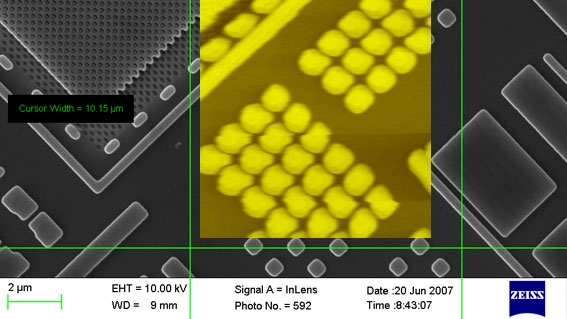 半導体構造を示すSEM像にAFM像を重ねたもの 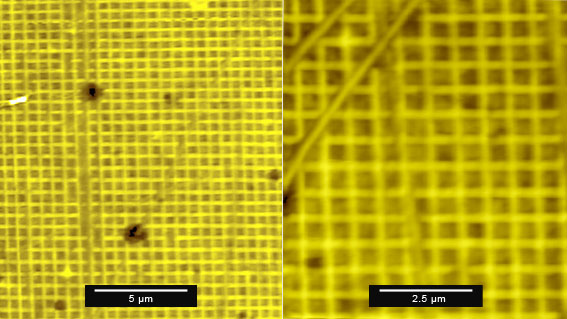 校正用試料のAFM像 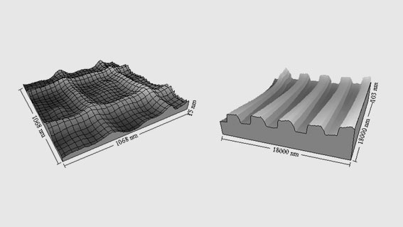 2種類の校正用試料の3D画像 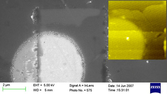 スパッタリングされたシリコン上の金のAFM像とSEM像の比較 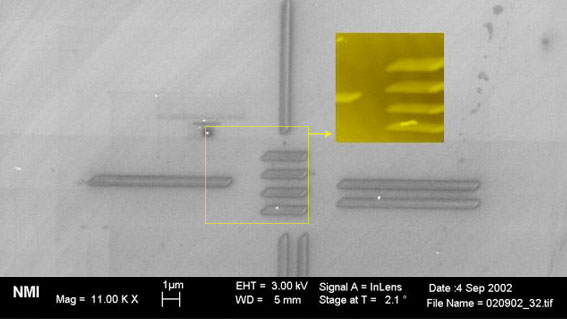 MEMS構造体のAFM像とSEM像の比較 |
紹介動画
|
[SuperFlat insitu AFM - imaging a calibration sample] [SuperFlat insitu AFM - imaging ZrO spheres] [SuperFlat insitu AFM - imaging a solar cell] [SuperFlat Atomic Force Microscope - combining AFM with SEM] |
Kleindiek社 <マイクロマニピュレータ・サブステージ>
▶ Kleindiek(クラインディーク)製品 トップページ
製品に関してのお問い合わせ